Layout
Tools used


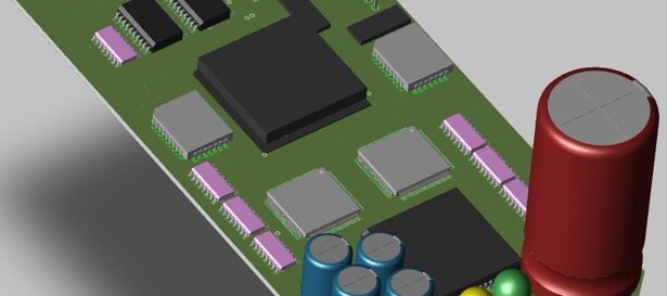
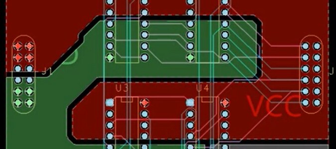
At OmCAD, we deliver precise, optimized PCB layouts that ensure performance, reliability, and manufacturability. Our engineers translate schematics into efficient board designs with optimized placement, routing, and signal integrity. Using advanced tools and best practices, we minimize noise, improve thermal performance, and meet strict design specs for diverse applications.
OmCAD specializes in designing precise component footprints from scratch, including complex and custom parts. We ensure accurate pad sizes, placement, and spacing in full compliance with IPC standards and manufacturer specs—guaranteeing reliability and compatibility during PCB assembly and manufacturing.
At OmCAD, PCB layout starts with precise component placement focused on signal integrity, thermal management, and space optimization. Our engineers strategically position components to reduce interference and boost performance—laying the groundwork for efficient routing and reliable functionality.
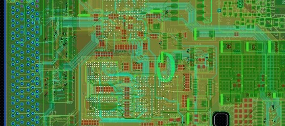
At OmCAD, trace routing is executed with exceptional accuracy and precision. Our engineers use advanced tools to optimize routing paths, minimize signal loss, and enhance overall performance. Through simulation and signal integrity analysis, we ensure high-speed designs meet the most demanding performance standards.
At OmCAD, we design PCB layouts with manufacturability in mind. By following DFM best practices, our engineers ensure efficient production while minimizing fabrication and assembly issues. Clear documentation and precise layout enable a smooth transition from design to manufacturing.
